
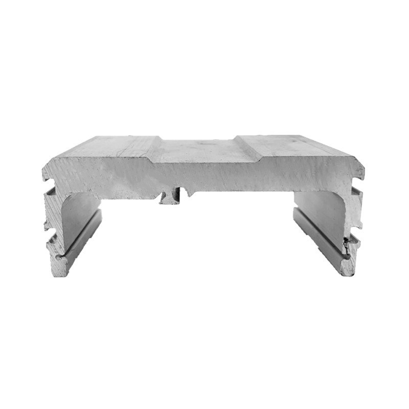
Custom Aluminum Profiles
Semiconductor Equipment Aluminum Profile - Die Opening
Profiles for wafer handling, AOI and EFEM frames: stress relieved for stability, conductive coating for charge control, cleanroom packed.
Product Details
Semiconductor equipment is the one place where an aluminium profile stops being a structural part and becomes part of the measurement chain. A wafer stage frame that moves 20 µm out of position ruins a lithography step. A particle shed from an anodised surface lands on a die. A frame that grows 100 µm between calibration and production shifts every coordinate the tool knows.
We open dies for sections used in wafer handling, AOI inspection, chip packaging and test, EFEM frames, and precision optical instruments. The tooling is ordinary extrusion tooling. What is different is the surface, the stress state and the cleanliness, and each of those changes the process rather than being added to it.
The three requirements that conflict
Semiconductor equipment asks for three things at once, and they pull against each other:
| Requirement | What drives it | What it conflicts with |
|---|---|---|
| Micron-level dimensional stability | Positioning accuracy over the tool's life | Thin walls and large sections, which are harder to stress relieve and quench evenly |
| Low particle and outgassing | Cleanroom class 10–1000, wafer contamination | Porous anodic coatings, which trap and release material |
| Static dissipation | Charge build-up attracts particles and can damage devices | Hard anodising, which is an excellent insulator |
The third row is the one that surprises designers who come from general industrial equipment. Hard anodising is normally sold as a premium finish — thick, hard, wear resistant. In a cleanroom it is a problem, because an insulating surface holds charge, and a charged surface attracts particles. That is why semiconductor frames are often specified with a conductive conversion coating rather than a thick anodic layer, and why the surface resistance value belongs on the drawing alongside the dimensional tolerances.
Surface finish decides particle performance
There is no such thing as a clean aluminium surface. There is a surface that releases little and one that releases a lot. The difference is chemistry and porosity, not cleanliness at the moment of packing.
Hard anodising builds a 25–50 µm porous oxide. The pores are useful — they accept dye, they hold lubricant, they resist wear — and they are also reservoirs. In a vacuum or a dry cleanroom, they can release adsorbed water and residues, and a damaged coating sheds oxide fragments.
Conductive conversion coating (chem-film type) is a thin, non-porous layer, typically well under a micron, that keeps surface resistance low enough to dissipate charge. It does not resist wear and it is not decorative. For a frame that never gets touched, that is the right trade.
Clean-grade anodising is a controlled anodic layer with sealing and a documented rinse sequence, used where wear resistance is needed and the part is not in the wafer environment.
Antistatic and low-outgassing coatings are used where the part sits close to the process. These are applied by specialist coaters and specified by outgassing test, not by description.
The practical rule: decide what the part touches. If it touches wafers or sits in the process environment, minimise the organic content and the porosity. If it only carries load and never enters the mini-environment, hard anodising is fine and cheaper.
Thermal expansion, and the frame that cannot be aluminium
Aluminium expands at 23.6 µm/m/K. Granite used for metrology frames and stages runs at 6–8. Steel is about 11.7. Invar is under 1.5.
That ordering explains a design rule that catches people late: a metrology loop should not run through aluminium. A 500 mm aluminium frame that shifts 5 °C moves 59 µm. If the same frame carries an encoder scale and a workpiece, both move together and the error cancels — that is fine. If the scale is on granite and the frame is aluminium, the differential is 39 µm over 500 mm for the same 5 °C, and no amount of machining tolerance fixes it.
So aluminium profiles in semiconductor equipment are usually used for structure and enclosure, not for the metrology loop: EFEM frames, equipment front-end structure, cover panels, cable management, non-critical mounting. Where they do enter a precision loop, the design has to be either short (so the expansion is small in absolute terms) or thermally controlled, or the aluminium has to be replaced by a low-expansion material.
This is worth raising early, because it is a design decision, not a manufacturing one. A supplier who promises to "hold ±0.01 mm" on a part that will be bolted to granite at a different temperature is promising something the material cannot deliver.
Specifications
| Item | Reference value |
|---|---|
| Applications | Wafer transfer, AOI inspection, packaging and test, EFEM frames, precision optics |
| Alloys | 6061-T6 precision grade; high-purity low-inclusion alloy; 6063-T5 for covers |
| Cross-section range | Circumscribed circle φ8 mm to φ300 mm |
| Wall thickness range | 0.6–5 mm |
| Critical assembly position tolerance | Reference ±0.02 mm |
| General dimensional tolerance | Reference ±0.05 mm |
| Straightness | Reference 0.2 mm/m |
| Flatness | Reference 0.03 mm / 100 mm |
| Parallelism | Reference 0.04 mm |
| Cleanroom compatibility | Class 10 to Class 1000 environment |
| Surface treatment | Clean-grade hard anodising, conductive conversion coating, antistatic coating, low-outgassing clean coating |
| Downstream processes | Ultra-precision CNC, micro-hole drilling, mirror polishing, cleanroom washing, vacuum clean packaging |
| CNC machining accuracy | Reference ±0.005 to ±0.01 mm |
| Maximum machined length | 6,500 mm |
| Die lead time | 7–10 days to sample for conventional sections |
| Batch lead time | 10–15 days after sample approval |
| Minimum batch | Tens of kilograms for R&D builds |
Stability: what a micron-level frame actually needs
A frame that has to hold position for years passes through four states, and each one moves it:
As quenched. Surface in compression, core in tension. Any machining releases part of that balance and the part bends. This is the biggest single source of a part that was good on the CMM and is out of position after assembly.
After aging. The precipitation reaction is mostly complete, but not entirely. Room-temperature aging continues slowly for months, which is why natural aging before machining matters: it lets the drift happen while the part still has machining stock on it.
After machining. Removing material from one face shifts the neutral axis and releases stress. A part machined symmetrically is more stable than one machined from one side only, and that is a design constraint as much as a process one.
In service. Thermal cycling at moderate temperature accelerates whatever relaxation remains. A frame cycled between ambient and 40 °C for a year will move more than the same frame held at constant temperature.
The process answer is the same four-step route used for any precision section: controlled quench, two-stage aging, deep cooling to about −80 °C, and 15–30 days of natural aging before the finish machining. For semiconductor work, we do not offer a shortcut on this. A part that moves after calibration costs the customer far more than the calendar time it saved.
Choosing the section for a wafer-handling frame
| Equipment | Where the profile goes | What the section must deliver |
|---|---|---|
| Wafer transfer | Equipment frame, transfer track, manipulator guide | Micron-level accuracy, very low internal stress, long-term stability |
| AOI inspection | Frame, optical platform profile | High flatness, low vibration, clean-compatible |
| Packaging and test | Structural members, test tooling profiles | Accuracy, low particle release, fast design iteration |
| Precision optics | Instrument frame, SEM matching structure | Flatness, low thermal expansion mismatch, clean surface |
| Etch and deposition | Frame, chamber support structure | Rigidity, corrosion resistance, clean fit |
| EFEM | Front-end module frame, wafer load structure | Accuracy, short lead time, clean fit |
Where it does not fit
- The metrology loop must be temperature-stable. Aluminium is the wrong material. Use granite, Invar or a thermally controlled structure; do not try to solve expansion with tolerance.
- You need a hard, wear-resistant and conductive surface at the same time. These are competing requirements. Conductive coatings are thin and soft; hard anodic layers are insulating. Choose which property the part actually needs.
- Your volume is a handful of units. Die cost plus a stress relief cycle plus cleanroom packaging is a lot of overhead for five parts. A machined part from plate may be the right answer.
- You need vacuum-compatible outgassing data for a specific coating. We can supply the base material and the dimensional data; coating outgassing certification depends on the coater and has to be specified with them, not assumed from the extrusion.
- The part has a deep narrow cavity or a closed undercut. Below about 0.6 mm wall and inside a small circumscribed circle, the die cannot reach, and the feature has to be machined.
- You need a fully documented cleanliness qualification with particle counts per part. We clean and pack to a cleanroom protocol; formal particle qualification of the assembled tool is the equipment builder's test.
What to send for a quote
Send the section drawing and the machined-part drawing, the datum scheme, the cleanroom class, the surface resistance requirement if there is one, the outgassing requirement if there is one, and the assembly temperature. If the part is part of a metrology loop, say so — it changes the recommendation, sometimes to a different material.
We will reply with the process route including the stress relief steps, the surface options that meet your cleanliness requirement, the tolerances we can confirm, and the honest position on anything the material cannot deliver. If aluminium is the wrong choice for the loop, that goes in the reply.
FAQ
How is a semiconductor equipment profile different from ordinary industrial profile?
Four things. The stress state is controlled through a full relief route, because a part that moves after calibration is worthless. The surface is specified by particle and outgassing behaviour, not by appearance. The dimensional tolerances are checked at a stated temperature, because 5 °C on a metre is 118 µm. And the part is washed and packed to a cleanroom protocol rather than wrapped in film.
What accuracy is possible?
Reference ±0.02 mm on critical assembly positions, ±0.05 mm on general dimensions, 0.03 mm/100 mm flatness, 0.04 mm parallelism and 0.2 mm/m straightness, with ±0.005 to ±0.01 mm after CNC finishing. These are capability references measured at 20 °C. The value on your order is set by your drawing, and we confirm in writing which critical dimensions we can hold before you order.
How is long-term dimensional stability achieved?
By the full route: controlled quench, two-stage aging, deep cooling to about −80 °C, and 15–30 days of natural aging before the final machining. Then by machining symmetrically and by rough machining, releasing, and finishing. None of these steps is optional on a part that has to hold a micron over a year.
How is cleanliness ensured?
Through the surface choice and the finishing sequence: a coating that does not trap material for parts near the wafer, ultrasonic washing after machining, a documented rinse, and vacuum-clean packaging. If you have a particle or outgassing specification, send it — the coating has to be selected against it, not described generically.
Why not use hard anodising everywhere for durability?
Because hard anodising is an insulator, and an insulating surface holds static charge that attracts particles. In a cleanroom that is a contamination source, not a durability benefit. For parts in the process environment, a conductive conversion coating is usually the better choice even though it wears faster. Where the part never enters the mini-environment, hard anodising is fine.
What is the lead time and the smallest batch?
Reference 7–10 days to die sample and 10–15 days for the batch after approval, plus the stress relief and aging time before machining. Tens of kilograms is workable for R&D builds. Be aware that a stabilised precision part is a matter of weeks rather than days, because the aging step is calendar time.
Can you supply material certificates and a dimensional report?
Yes: mill certificate with heat number, chemical composition, mechanical properties, and a CMM dimensional report against your datum with the measurement temperature recorded. If your quality system needs an accredited third-party certificate or a witnessed inspection, tell us at enquiry — it is arranged separately and affects the schedule.
Send your drawing
Email the section and machined-part drawings, the datum scheme, the cleanroom class and the surface requirement to linjunbing@truetrustlv.com, or send them on WhatsApp at +86 136 6644 0600. You will get a process route, a surface recommendation and a written tolerance statement.
GET A QUOTE
Once you have submitted your requirements, we will contact you as soon as possible regarding your product inquiry.:Semiconductor Equipment Aluminum Profile - Die Opening