Custom Aluminum Profiles
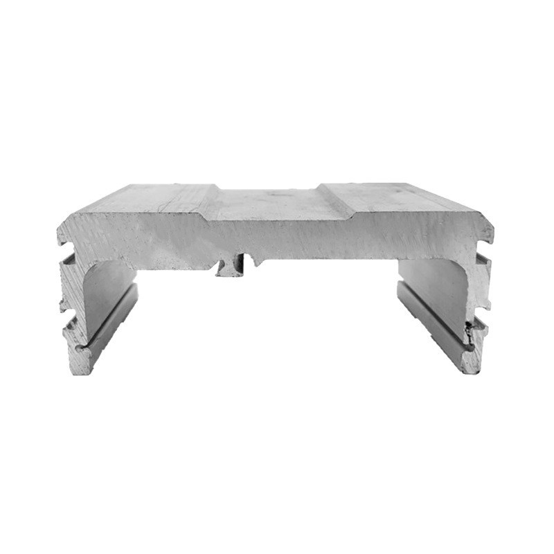
Semiconductor equipment aluminum profile mold opening
Semiconductor equipment manufacturing is the pinnacle of precision manufacturing. Semiconductor equipment such as wafer
Product Details
Semiconductor equipment manufacturing is the pinnacle of precision manufacturing. Semiconductor equipment such as wafer transfer systems, optical inspection equipment, and chip packaging and testing equipment have far more stringent requirements for the accuracy, cleanliness, and long-term stability of aluminum profile structural components than ordinary industrial equipment. In equipment such as etching machines and deposition equipment, aluminum and aluminum alloys typically account for 30%-50% of metal materials. As a core frame material for semiconductor equipment, aluminum profiles must meet four standards simultaneously: micron-level accuracy, extremely low internal stress, cleanliness without particle precipitation, and long-term dimensional stability.
Shanghai Chuansi Aluminum focuses on the stringent requirements of semiconductor equipment for aluminum profiles, providing a one-stop service for the entire process, from ultra-precision mold design, high-precision extrusion molding, ultimate stress relief treatment to clean-grade surface treatment and dust-free packaging. Wafer transfer equipment frames require profiles to have extremely high rigidity and micron-level positioning accuracy; The AOI optical inspection equipment frame requires extremely high profile flatness to ensure clear imaging of the optical system; The structural components of chip packaging testing equipment require low particle precipitation and are suitable for a clean environment.
01 Quality starts with raw materials
Ultra-high purity aluminum alloy produced using A00 virgin aluminum ingots, containing no waste aluminum, with pure materials and dense structure. Various materials can be selected according to the specific requirements of semiconductor equipment, such as 6061-T6 ultra-high-precision aluminum alloy (mainstream semiconductor equipment structural components), high-purity impurity-free aluminum alloy (front-end process sensitive to metal ions), and 6063-T5 precision aluminum alloy (optical instrument frame).
02 Ultra-precision molds and micron-level precision control
Semiconductor equipment requires a much higher level of accuracy than ordinary industrial equipment. Using imported high-end mold steel, the mold cavity accuracy can reach ±0.01mm through slow wire precision machining and mirror polishing process. Equipped with a high-precision extrusion production line and an online laser inspection system, the profile dimension fluctuations are controlled in real time throughout the entire process, and the tolerance of key assembly positions can be stably controlled within ±0.02mm. Straightness ≤ 0.2 mm/m, flatness ≤ 0.03 mm/100 mm, parallelism ≤ 0.04 mm. The flatness error in the wafer transfer area can be controlled within ±0.1mm/m, meeting the requirements of the SEMI international standard.
03 Ultimate stress relief, eliminating precision drift
When semiconductor equipment operates for a long time, the residual stress inside the profile will gradually be released, leading to slight dimensional changes, which directly affects the accuracy of wafer transport and positioning and the accuracy of detection. The ultimate stress relief process of "quenching + two-stage aging + cryogenic treatment + natural aging" is adopted to eliminate the residual stress inside the profile to the greatest extent possible, and the internal stress level is far lower than the conventional industry standard. The profiles undergo minimal deformation after precision machining, maintain stable dimensions under constant temperature and clean environments for a long time, and eliminate equipment accuracy drift caused by stress release.
04 Clean-grade surface treatment and dust-free packaging
Semiconductor equipment operates in cleanrooms, which have stringent requirements for particle precipitation, VOC release, and ease of cleaning on the surface of aluminum profiles. It can provide a variety of semiconductor-grade surface treatment solutions such as clean-grade hard anodic oxidation, conductive oxidation, antistatic coating, and low-precipitation clean coating. The film layer is dense and pore-free, low particle precipitation, has extremely low VOC emission, and the surface is smooth and easy to clean and disinfect. All deep-processed finished products undergo dust-free cleaning and vacuum clean packaging to avoid secondary pollution during transportation.
05 Adapting to the R&D pace of the semiconductor industry
Deeply adapted to the characteristics of the semiconductor and precision instrument industry, characterized by "high degree of customization, rapid R&D iteration, and small order volume," it provides dedicated R&D customization channels, prioritizes production for small-batch precision orders, and quickly responds to new product testing and iteration needs. We can assist customers in providing full-process technical support, including material selection, structural optimization, and cleanliness performance verification.
Processing capacity parameters:
| Project | Parameters / Description |
|---|---|
| Applicable scenarios | Wafer transfer equipment, AOI optical inspection equipment, chip packaging testing equipment, precision optical instruments |
| Optional materials | 6061-T6 ultra-high-precision aluminum alloy, high-purity impurity-free aluminum alloy, 6063-T5 precision aluminum alloy |
| Execution Standards | GB/T 6892-2023 Technical Specification for Clean Materials for Ultra-high Precision and Semiconductor Equipment |
| cross-sectional range | Circumscribed circle φ8mm-φ300mm |
| wall thickness range | 0.6mm-5mm |
| Critical assembly position tolerance | ≤±0.02mm |
| conventional bit tolerance | ±0.05mm |
| straightness | ≤0.2mm/m |
| flatness | ≤0.03mm/100mm |
| parallelism | ≤0.04mm |
| cleanliness level adaptation | Class10-Class1000 Clean Environment |
| surface treatment | Clean grade hard anodic oxidation, conductive oxidation, antistatic coating, low precipitation clean coating |
| deep processing supporting equipment | Ultra-precision CNC machining, micro-hole machining, mirror polishing, dust-free cleaning, vacuum clean packaging |
| CNC machining accuracy | ±0.01-0.005mm |
| Maximum machining length | 6500mm |
| mold opening cycle | Sampling for conventional structures takes 7-10 days. |
| Batch delivery time | 10-15 days after sample confirmation |
| minimum order quantity | Supports tens of kilograms of R&D prototyping |
| Production origin | Shanghai Qingpu |
Typical application scenarios of aluminum profiles for semiconductor equipment:
| Equipment Type | application site | Key Requirements |
|---|---|---|
| wafer transfer apparatus | Equipment frame, transmission track, manipulator guide rail | Micron-level accuracy, extremely low internal stress, long-term dimensional stability |
| AOI optical detection apparatus | Detection equipment frame, optical platform profile | Ultra-high flatness, low vibration, suitable for clean environments |
| chip packaging test equipment | Packaging equipment structural components, testing tooling profiles | High precision, low particle precipitation, rapid iterative adaptation |
| Precision optical instruments | Optical instrument frame and electron microscope matching structure | Ultra-high flatness, low thermal expansion, clean surface |
| Etching/Deposition Equipment | Equipment frame and cavity support structure | High rigidity, corrosion resistance, clean fit |
| EFEM Device Framework | Equipment front-end module frame and wafer loading structure | High precision, fast delivery, clean fit |
Typical application scenarios:
semiconductor wafer transfer equipment profile
AOI optical inspection equipment framework
chip package testing equipment structural component
wafer handling robot guide rail
EFEM Device Framework
precision optical instrument rack
Electron microscope matching structural parts
Etching/Deposition Equipment Frame
high-precision inspection of tooling profiles
semiconductor cleanroom equipment rack
FAQ (Frequently Asked Questions)
Q1: What are the differences between aluminum profiles for semiconductor equipment and ordinary industrial aluminum profiles?
A: There are five core differences between aluminum profiles for semiconductor equipment and ordinary industrial aluminum profiles: First, the precision requirements are different—the tolerance of key assembly positions for semiconductor equipment is ≤±0.02mm, while ordinary industrial profiles are usually ±0.05mm to ±0.1mm; Secondly, the cleanliness requirements are different—semiconductor equipment needs to be adapted to a Class 10-Class 1000 clean environment, with low particle precipitation and low VOC emission; Third, the dimensional stability requirements are different—ultimate stress relief treatment is needed to ensure long-term dimensional stability; Fourth, the surface treatment requirements are different—special treatments such as clean-grade anodic oxidation, conductive oxidation, and antistatic coating are required; Fifth, the quality system requirements are different—they must comply with the technical specifications for clean materials for semiconductor equipment. In equipment such as etching machines and deposition equipment, aluminum and aluminum alloys typically account for 30%-50% of metal materials.
Q2: How accurate can aluminum profiles for semiconductor equipment be?
A: The dimensional tolerance of key assembly positions is ≤±0.02mm, the mold cavity accuracy can reach ±0.01mm, the straightness is ≤0.2mm/m, the flatness is ≤0.03mm/100mm, the parallelism is ≤0.04mm, and the CNC machining accuracy is ±0.01-0.005mm. The flatness error in the wafer transfer area can be controlled within ±0.1mm/m, meeting the requirements of the SEMI international standard. The AOI optical inspection equipment frame requires extremely high profile flatness to ensure clear imaging of the optical system.
Q3: How can aluminum profiles for semiconductor equipment ensure long-term dimensional stability?
A: Through the ultimate stress relief process of "quenching + two-stage aging + cryogenic treatment + natural aging", the residual stress inside the profile is eliminated to the greatest extent possible, and the internal stress level is far lower than the conventional industry standard. The profiles undergo minimal deformation after precision machining, maintain stable dimensions under constant temperature and clean environments for a long time, and eliminate equipment accuracy drift caused by stress release. In semiconductor devices, the long-term dimensional stability of aluminum profiles is a more important core indicator than the initial accuracy.
Q4: How can the cleanliness of aluminum profiles for semiconductor equipment be ensured?
A: Cleanliness is ensured through four steps: First, a clean-grade surface treatment solution—clean-grade hard anodic oxidation, conductive oxidation, antistatic coating, and low-precipitation clean coating, with a dense film layer without pores and low particle precipitation; Second, processing environment control – key processing steps are carried out in a clean environment; Third, dust-free cleaning – all deep-processed finished products undergo dust-free cleaning to remove processing residues; Fourth, vacuum clean packaging – vacuum packaging immediately after cleaning to avoid secondary contamination. It can be adapted to Class10-Class1000 clean environments.
Q5: What is the mold opening cycle and minimum order quantity for aluminum profiles for semiconductor equipment?
A: The conventional structural mold opening cycle is 7-10 days for sample production, and 10-15 days after batch delivery sample confirmation. It supports tens of kilograms of R&D prototyping, adapts to the characteristics of the semiconductor industry of "high degree of customization, rapid R&D iteration, and small order volume", and prioritizes production for small-batch precision orders. Sampling for ordinary precision grade (tolerance ±0.05mm) takes 7-8 days; Ultra-high precision (tolerance ≤±0.02mm) sampling takes 8-10 days; Samples of ultra-high-precision cross-sections with complex structures such as multiple cavities and microgrooves will be produced in 10-12 days.
GET A QUOTE
Once you have submitted your requirements, we will contact you as soon as possible regarding your product inquiry.:Semiconductor equipment aluminum profile mold opening